
As a civil engineering scholar, I had the chance to discover numerous branches of engineering, together with electrical engineering. Throughout this journey, I used to be launched to printed circuit board (PCB) design, and I used to be fascinated by the method of making circuits and understanding how every part works collectively to type a practical design.
I shortly realized that selecting the finest PCB design software program is essential to making sure environment friendly, dependable, and high-quality designs. The best software program streamlines the design course of, supplies strong instruments for routing, simulating, and validating circuits, and helps handle complexity whereas guaranteeing the ultimate product meets all technical necessities.
Quick-forward to in the present day, I’ve evaluated a variety of PCB design software program instruments to judge their efficiency, usability, and options. With quite a few choices obtainable, it was important for me to delve into every software’s capabilities and assess how they deal with real-world initiatives.
By mixing skilled opinion with priceless suggestions from G2 customers, I’ve compiled a listing of the 7 finest PCB design software program that will help you discover the perfect match to your personal initiatives.
7 finest PCB design software program: My picks for 2025
-
Altium Designer: Finest for superior design instruments and an intensive part library
Affords highly effective structure and schematic instruments for skilled PCB design. ($355/month) -
Altium 365: Finest for PCB structure modifying and 3D visualization
Allows collaborative design with cloud-based 3D visualization. (price relies on the connectors chosen) -
PADS Skilled: Finest for advanced PCB layouts and superior routing
Handles high-density designs with precision routing capabilities. ($286.92/month) -
Allegro PCB Designer: Finest for high-density designs and error correction
Supplies strong instruments for managing large-scale, advanced PCBs. (pricing obtainable on request) -
Autodesk Fusion: Finest for built-in mechanical and electrical design
Combines PCB design with 3D modeling and mechanical integration ($85/month)
-
Altium CircuitMaker: Finest community-driven, open-source PCB design software
Free platform that fosters collaboration amongst hobbyists and professionals. (free) -
Autodesk EAGLE: Finest for intuitive interface and schematic seize
Simplifies PCB design with user-friendly schematic and structure instruments. (pricing obtainable on request)
* These PCB design software program are top-rated of their class, in response to G2’s 2025 Winter Grid Report. I’ve additionally added their month-to-month pricing to make comparisons simpler for you.
My high 7 finest PCB design software program suggestions for 2025
PCB design software program is a strong software used to create and optimize printed circuit board layouts. It helps engineers design the digital circuits that type the spine of recent units.
As I explored the perfect PCB design software program, I discovered that they provide greater than fundamental structure capabilities. They supply superior options like real-time collaboration, 3D visualization, and error-checking. The worldwide PCB design software program market is projected to develop from $4.12 billion in 2025 to $13.32 billion by 2034, reflecting a sturdy demand for these instruments
Evaluating numerous instruments with professionals on small initiatives allowed me to establish options that improved the design course of whereas additionally serving to me relive my engineering days. On this article, I’ll spotlight what made these instruments stand out and the way they helped me overcome frequent design challenges.
How did I discover and consider the perfect PCB design software program?
I began by reviewing G2’s newest Grid Studies to establish which PCB design software program platforms constantly excel in usability, function completeness, and general satisfaction. This gave me a powerful baseline of trusted instruments {that electrical} engineers already depend on.
From there, I narrowed my record by getting hands-on expertise with the options and workflows. For options the place direct testing wasn’t absolutely potential, I leaned on verified G2 consumer suggestions, product demos, and vendor documentation to know real-world efficiency and limitations. I additionally used AI-powered evaluation to scan 1000’s of consumer opinions, surfacing frequent reward factors and recurring frustrations.
All through testing, I targeted on the expertise from an engineer’s perspective: Was the platform intuitive? Did it simplify PCB structure, optimization, and administration? Might it deal with advanced designs and not using a steep studying curve? And most significantly, would it not combine easily into present engineering workflows?
Screenshots on this article mix my testing visuals with verified vendor photos from G2.
What I search for in PCB design software program
When evaluating PCB design instruments, I take into account options that streamline the design course of, improve effectivity, and make sure the creation of high-quality, dependable circuits:
- Superior routing capabilities are important for advanced designs. The software program ought to enable for fast computerized routing of traces, particularly in multi-layer PCBs, nevertheless it should additionally let me make guide changes to fine-tune the sign paths. It ought to deal with layer transitions easily, routing indicators by way of interior layers utilizing vias. Through stitching is vital for creating a good floor or energy aircraft, which helps scale back noise and enhance sign high quality. The software program must also assist impedance-controlled routing to make sure the traces meet particular impedance necessities, which is essential for high-speed circuits. Lastly, it ought to let me modify hint width and clearance to satisfy manufacturing and electrical requirements.
- Design rule checks (DRC) are important for me to establish potential design errors earlier than shifting into manufacturing. The software program I take advantage of should present customizable DRC settings that assist examine for violations of design constraints like hint width, pad sizes, by way of dimensions, and clearance between traces, pads, and vias. I would like to have the ability to create guidelines based mostly on the fabrication capabilities of the PCB producer, equivalent to minimal hint width and most current-carrying capability. The software program ought to robotically flag errors like hint overlap, unconnected nets, or part misplacement and generate an easy-to-read report for additional evaluation so I can deal with points early.
- Electrical rule checks (ERC) are simply as vital to make sure the circuit features accurately. ERC helps me catch points associated to {the electrical} connectivity of elements and indicators, equivalent to unconnected nets, energy/floor shorts, and incorrect part values. The software program should be certain that all elements are linked as proven within the schematic and that no unintended electrical paths are created. For instance, it ought to examine for floating pins on built-in circuits (IC), mismatched energy rails, and incorrect internet assignments. In high-speed designs, ERC must also be able to figuring out potential sign integrity points, equivalent to unbalanced differential pairs and floor bounce, which might have an effect on circuit efficiency.
- Assist for multi-layer PCB designs, particularly for high-density or high-performance purposes, multi-layer PCBs are sometimes required. The software program I take advantage of ought to enable for the seamless creation of four-layer, six-layer, or much more advanced designs. It’s vital for me to have the ability to outline layer stacks, with interior layers used for routing and outer layers for part placement. The software should additionally assist energy and floor planes to make sure electrical stability by minimizing electromagnetic interference (EMI). Moreover, the flexibility to deal with blind vias (vias that don’t undergo all layers) and buried vias (vias that solely join interior layers) is essential for maintaining the design compact. The software program must also robotically optimize the routing between layers and effectively handle each sign integrity and energy integrity in multi-layer configurations, which is essential for high-quality, dependable designs.
- Sign integrity evaluation is essential for me to guarantee that high-speed indicators are transmitted without degradation. The software I take advantage of must come outfitted with SI simulation tools that analyze factors like trace impedance, sign reflection, crosstalk, and electromagnetic interference (EMI). These tools assist me understand the way indicators behave on the PCB and guarantee they stay dependable, particularly in advanced designs. Features like sign path evaluation and eye diagrams are essential as a result of they enable me to visualize the quality of sign transmission and examine for any points that might affect efficiency. This provides me confidence that the design will meet the required sign integrity standards.
- Having a complete part library is a large time-saver for me. The software program ought to include a variety of frequent elements, every together with correct footprints, symbols, and 3D fashions, which makes it a lot simpler to get began with no need to manually create every half. When working with customized elements, the software program should enable me to simply create and modify footprints and symbols, which helps me outline vital parameters like pad dimension, gap diameter, and pitch. This ensures that each one elements match accurately on the PCB.
- 3D visualization is invaluable for verifying the bodily layout of the PCB. This function lets me view the PCB in three dimensions to establish potential mechanical conflicts, equivalent to elements which will collide with the enclosure or different elements of the design. It helps confirm part orientation and clearances between elements and traces. Moreover, the flexibility to simulate meeting in 3D can be certain that all elements match as meant earlier than manufacturing, stopping pricey redesigns. The 3D mannequin additionally aids in confirming the mechanical integrity of the board, guaranteeing there’s satisfactory stiffness and assist for elements which will expertise bodily stress throughout operation.
- Collaboration instruments are essential when working in a team environment. I search for software that supports cloud-based design sharing, permitting for seamless real-time collaboration amongst team members, no matter location. The ability to implement model control within the design tool is vital for tracking adjustments and preventing accidental overwrites of critical data. I want tools that enable comments and annotations within the design information so that the entire team can focus on and resolve points directly within the software. This feature is particularly helpful for teams that work in iterative design cycles or when integrating suggestions from numerous stakeholders. Design history tracking ensures that I can revert to earlier variations of the design if crucial.
The record under incorporates real consumer opinions from our greatest PCB design software program class web page. To qualify for inclusion within the class, a product should:
- Modify PCB layouts and PCB circuitry
- Embrace a elements library so customers can simply implement high-quality PCB footprints
- Present schematic modifying instruments for modification {of electrical} properties and different attributes of elements, wires, nets, and pins.
This knowledge has been pulled from G2 in 2025. Some opinions have been edited for readability.
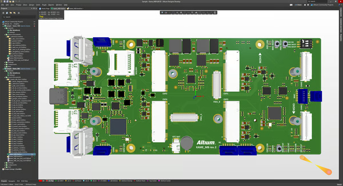
1. Altium Designer: Finest for superior design instruments and an intensive part library
Altium Designer provides a unified platform that integrates totally different design instruments, together with schematic seize, structure routing, documentation, and simulation, into one atmosphere. What I respect most is the flexibility to seamlessly transfer between these phases. For instance, as soon as somebody creates the schematic diagram, they’ll simply transition to the layout-routing part, adjusting the design whereas visualizing the ultimate product.
A function that basically impressed me is design for manufacturing (DFM). This ensures that designs are usually not solely practical but in addition simple to supply. The DFM instruments assist establish potential points early within the course of, decreasing errors and saving time through the manufacturing part. Groups I labored with talked about that it was reassuring for them to know that their design is optimized for manufacturing earlier than shifting on to precise fabrication.
With the 3D flex-rigid design, I noticed that groups might visualize how the totally different layers of a PCB interacted, together with each versatile and inflexible elements. This was particularly helpful when working with extra advanced, multi-layered designs. I can see how seeing how every part interacts in 3D can provide producers higher perception and assist them make extra knowledgeable choices whereas routing the structure.
Its intensive part library provides an unlimited choice of elements, elements, and templates, permitting groups to shortly discover what they want. This function reduces the necessity to manually design elements from scratch, and groups can use pre-validated elements that assist reduce errors. I noticed how the good selection makes the method sooner and extra dependable, which is at all times a plus. In keeping with G2 Knowledge, 83% customers love its part libraries.
The largest side I observed pertains to system necessities. Altium Designer performs exceptionally effectively on high-end machines, nevertheless it does require substantial reminiscence and processing energy. From what I gathered in G2 opinions, on much less highly effective computer systems, there will be some slowdowns with bigger, extra advanced initiatives. Even so, the software program stays very succesful for detailed PCB design.
One other space to notice is including footprints to units. Whereas Altium provides an intensive library, discovering the precise footprint can contain navigating a number of libraries. Linking the footprint to the schematic image isn’t at all times instantly intuitive, and verifying accuracy can take a number of further steps. Regardless of these minor inconveniences, the system nonetheless permits exact and dependable part placement as soon as conversant in the workflow.
I additionally gathered from G2 opinions that the training curve will be steep for newcomers. Altium Designer is filled with options, which is a large benefit for skilled customers, although it might take a while to get snug with all of the instruments. When you’re acquainted, the platform’s depth and suppleness actually shine, making it a strong selection for skilled PCB design.
What I like about Altium Designer:
- From what I collect from G2 opinions, the unified platform of Altium Designer makes it simple for PCB groups to maneuver seamlessly between design phases, from schematic seize to structure routing.
- The DFM function actually impressed me by serving to optimize designs for manufacturing. It allowed groups to establish potential points early, scale back errors, and make sure the design was prepared for fabrication.
What G2 customers like about Altium Designer:
“Altium Designer supplies all the things wanted for design and structure in a single software, eliminating the necessity for extra purchases. It integrates seamlessly with large-part databases, providing pricing, availability, and environment friendly manufacturing BOM technology. The built-in SPICE software helps analog simulation, and its structure options embody matched size routing, managed impedance, differential pairs, and each guided guide and auto-routing, which save important time as soon as mastered. The mixing of 3D mechanical fashions into designs and outputs for mechanical use is extremely helpful. General, Altium Designer is the perfect digital design software I’ve ever used.”
– Altium Designer Overview, Tim T.
What I dislike about Altium Designer:
- I observed that Altium Designer calls for substantial reminiscence and processing energy. From what I noticed in G2 opinions, much less highly effective computer systems can expertise slowdowns with bigger initiatives, although on high-end machines, efficiency stays easy.
- Including footprints to units could be a bit cumbersome. I discovered that navigating a number of libraries and linking footprints to schematic symbols isn’t at all times intuitive — some extent a number of G2 reviewers additionally highlighted, however when you get the dangle of it, part placement turns into exact and dependable.
What G2 customers dislike about Altium Designer:
“One space for enchancment is including extra options to the “Producer Half Search.” Moreover, navigating the software program and not using a mouse will be difficult, particularly when utilizing a laptop computer. Proper-clicking and dragging on a trackpad will be irritating, although that’s partly as a result of laptop computer design. One other suggestion pertains to defining board dimension; as an example, once I wanted a board that was precisely 50mm x 50mm, it was laborious to attract exact traces. I ended up setting the grid dimension to 1mm and estimating the size. It could be useful to have a function that shows the size of line drawings or the size of the shapes being created.”
– Altium Designer Overview, Trevor M.
2. Altium 365: Finest for PCB structure modifying and 3D visualization
One of Altium 365‘s standout options is its real-time collaboration capabilities. From many G2 opinions, I observe that it has helped many circuit groups work on the identical designs concurrently. Whether or not reviewing schematics or making PCB structure changes, it ensured everybody was on the identical web page. The platform’s model management system ensures that each change is tracked, which permits groups to view revision histories or roll again to earlier variations with ease.
It has extremely environment friendly undertaking administration instruments which have made dealing with advanced designs a lot simpler, particularly when engaged on intricate designs. I discovered the method of making and modifying elements to be each intuitive and highly effective, permitting for detailed work with out feeling overwhelming. I can see how this flexibility can be an enormous asset for groups, enabling them to handle large-scale initiatives with ease.
I’ve additionally gathered from G2 opinions how newcomers loved working with the PCB structure editor. It’s extremely customizable, which permits groups to make changes to designs shortly and seamlessly. I actually appreciated the flexibility to effortlessly transition between schematic and PCB. It might save groups plenty of time, as they’ll shortly modify and export designs. For groups that have to combine these adjustments into their bigger platform-based initiatives, I imagine that this function would make all the course of far more environment friendly.
The 3D visualization function was one other space the place Altium 365 impressed me. I might visualize how elements match on the board with ease, particularly in tight areas. The software program’s assist for .step 3D our bodies made it simple to see how all the things would match collectively. What stood out was the 3D rendering pace – even when working with advanced elements, they rendered shortly with none noticeable lag. I discovered the “snap factors” function significantly helpful, because it helped PCB groups place even probably the most awkward 3D our bodies with nice precision.
Lastly, the draftsman software has been an absolute spotlight. Producing high-quality meeting drawings was a breeze with just some clicks. This software allowed G2 customers to create detailed and visually interesting drawings, which I might think about can be very helpful for manufacturing groups that want clear documentation for meeting.

Nevertheless, regardless of these optimistic experiences, I observed a number of areas the place PCB routing guidelines could possibly be improved. Setting them up generally required a little bit of programming information, which is perhaps difficult for newcomers. A extra user-friendly interface for configuring these guidelines would make the method smoother; nonetheless, as soon as conversant in the foundations system, it supplies exact management over design constraints.
One other side is the design rule system. Some customized queries, like organising guidelines to disregard interfering elements, didn’t at all times behave constantly. As an illustration, a “part clearance” rule may not at all times ignore collisions. Whereas this has been reported by a number of G2 customers, the system nonetheless permits advanced guidelines to be utilized successfully as soon as correctly configured.
I additionally noticed that monitor size calculation might sometimes be inconsistent. Sure small segments on particular layers had been generally ignored, which might have an effect on impedance-controlled designs. Even so, the platform typically permits correct monitor administration for most traditional layouts.
Lastly, the Invoice of Supplies (BOM) function can take a bit longer to generate and requires updating after schematic adjustments. Whereas this provides some further steps, it ensures that the BOM stays correct and displays all design modifications, which is essential for exact manufacturing and meeting.
What I like about Altium 365:
- Altium 365’s undertaking and library administration instruments made dealing with advanced designs a lot simpler for PCB groups. Its intuitive and highly effective options allowed detailed work with out feeling overwhelming, which might be priceless for groups managing large-scale initiatives.
- The 3D visualization function impressed me, because it allowed customers to shortly see how elements match on the board, even in tight areas. Quick rendering and exact placement utilizing the “snap factors” function enormously enhanced the design course of.
What G2 customers like about Altium 365:
“What I like most about Altium 365 is how effortlessly it permits cloud-based collaboration, making it splendid for real-time PCB design initiatives, particularly for worldwide groups. Its seamless integration with Altium Designer and the flexibility to entry designs from wherever make it my go-to software, one I take advantage of virtually day by day. For these utilizing model management instruments like Git, the centralized library administration and reusable design choices considerably pace up improvement. The intuitive interface turns into simple to navigate with some preliminary exploration, making it sensible for almost any PCB undertaking. Plus, the rising group assist is invaluable.”
– Altium 365 Overview, Angel O.
What I dislike about Altium 365:
- I observed that organising PCB routing guidelines can generally require programming information, which isn’t beginner-friendly. A number of G2 reviewers talked about the identical, although when you’re acquainted, the system nonetheless provides exact management over design constraints.
- The design rule system isn’t at all times constant, guidelines like “part clearance” don’t behave completely each time. I noticed this mirrored in a number of G2 opinions, however as soon as configured accurately, it nonetheless permits advanced guidelines to be utilized successfully.
What G2 customers dislike about Altium 365:
“The software program will be gradual to start out and entry information, particularly over a community. Some default settings, just like the connection matrix, generate pointless warnings that make it tougher to establish actual points. The Invoice of Supplies function takes time to generate and requires updates when adjustments are made to the schematic. Moreover, the software program slows down with bigger designs, and whereas it integrates effectively with third-party elements, occasional points with mismatched footprints or image requirements can come up.”
– Altium 365 Overview, Hemant A.
3. PADS Skilled: Finest for advanced PCB layouts and superior routing
One of many greatest strengths I observed about PAD Skilled is its capacity to deal with advanced PCB layouts. This function was significantly helpful when groups I labored with created intricate designs requiring exact management.
The interactive options, particularly the auto-routing choices, really stood out to me. They considerably sped up the structure course of, and groups might visually monitor the routing because it progressed, making all the course of smoother and extra environment friendly.
One other standout side is the intensive documentation. From many opinions, I gathered that G2 customers relied closely on the documentation firstly, and it did not disappoint. It lined all the things from fundamental performance to extra superior choices, serving to groups shortly perceive options that might have in any other case been difficult to determine.
I additionally appreciated the schematic half view, which helps you to rotate elements at totally different angles. This was a surprisingly useful function, making it simpler to visualise and work with incessantly used elements, particularly those who want particular orientations. In keeping with G2 Knowledge, 82% customers reward its schematic editor.
One of the vital spectacular integrations I got here throughout was the hyperlink to HyperLynx for sign integrity or energy Integrity simulations. I noticed how effortlessly it might carry out detailed simulations, and the seamless integration actually enhanced the software’s capabilities.

The versatile design constraint system allowed customers to simply outline particular design guidelines, including precision to designs and guaranteeing compliance with manufacturing necessities. I did discover, nonetheless, that G2 customers talked about this function could possibly be much more highly effective if paired with improved usability for template creation, although it nonetheless supplies robust management over design constraints.
I additionally discovered that the preliminary setup might really feel a bit overwhelming. The software provides many options, and getting it up and operating isn’t so simple as some customers would possibly hope. A extra streamlined setup course of might assist, however as soon as configured, the platform features successfully.
Many customers famous that whereas the GUI works, the interface feels considerably outdated in comparison with fashionable PCB design instruments. After analyzing a number of G2 opinions, I noticed that whereas the software is absolutely practical, a extra intuitive and visually partaking interface might improve navigation, although the core performance stays strong.
One other level is dashboard efficiency. For some designs, computing and processing evaluation can take longer than anticipated. Even for easy initiatives, this wait can really feel noticeable, although it doesn’t have an effect on the accuracy or general usefulness of the evaluation.
I additionally found, from G2 opinions, that constraint supervisor template creation and reuse could possibly be extra intuitive. Whereas the system is versatile, creating and reusing templates can really feel cumbersome. Bettering this workflow would improve consumer expertise, however the present system nonetheless permits exact constraint administration.
Lastly, assist for importing legacy designs could possibly be extra strong. Importing older designs might take further time, which could possibly be a minor ache level for customers transitioning from different instruments. Even so, the platform supplies ample performance to deal with legacy initiatives successfully as soon as imported.
What I like about PADS Skilled:
- The flexibility to deal with advanced PCB layouts was a game-changer, particularly when engaged on intricate designs requiring exact management. This function makes the software extremely efficient for detailed initiatives.
- I famous from numerous opinions that seamless integration with HyperLynx for Sign and Energy Integrity simulations gave customers entry to superior evaluation capabilities, enhancing designs with highly effective insights.
What G2 customers like about PADS Skilled:
“It is very useful for backend design and extremely dependable with glorious accuracy. The consumer interface is supportive {and professional}, making it simple to make use of repeatedly for designing and analyzing PCB fabrication. Integration is easy, and the shopper assist from Mentor Graphics is excellent. General, it is simple to implement.”
– PADS Skilled Overview, Subhadeep P.
What I dislike about PADS Skilled:
- I observed that the preliminary setup can really feel a bit overwhelming. A number of G2 reviewers talked about this as effectively, although as soon as configured, the platform works successfully and supplies robust management over design constraints.
- Creating and reusing constraint supervisor templates isn’t at all times intuitive. I noticed the identical level highlighted in a number of G2 opinions, however regardless of the additional steps, the system nonetheless permits exact template administration when you get the dangle of it.
What G2 customers dislike about PADS Skilled:
“One draw back of utilizing PADS Skilled is that it takes a big period of time to course of and compute analyses, even for one thing so simple as the dashboard, which will be fairly irritating.”
– PADS Skilled Overview, Souvik G.
4. Allegro PCB Designer: Finest for high-density designs and error correction
I just lately explored Allegro X PCB Designer, and I discovered it distinctive for creating CPU motherboards and dealing with high-density interconnect (HDI) PCB designs.
Its capacity to develop compact, space-efficient electronics whereas sustaining superior performance is spectacular. From G2 consumer opinions, I noticed that the software makes it potential to pack intricate elements into smaller areas, a function that basically stood out to me and felt like a big benefit for contemporary electronics design.
Certainly one of my favourite options is the error correction system for schematic design. With its three-step course of, it made guaranteeing schematic accuracy really feel intuitive and easy for professionals. I observed throughout a number of opinions that it flagged errors early, corrected them logically, and validated the outcomes systematically, streamlining the design course of and minimizing potential errors.
I additionally appreciated the pre-analysis and post-analysis capabilities, which allowed customers to catch and resolve points each earlier than and after the design part, making all the workflow extra environment friendly and dependable.
I used to be additionally impressed by Allegro’s versatile workspace, This adaptability was an enormous plus for PCB administration groups, because it made staying organized and productive a lot simpler. Aligning the software’s setup with design habits felt like an effective way to enhance effectivity and luxury.

The versatile design constraint system allowed customers to simply outline particular design guidelines, including precision to designs and guaranteeing compliance with manufacturing necessities. I did discover, nonetheless, that G2 customers talked about this function could possibly be much more highly effective if paired with improved usability for template creation, although it nonetheless supplies robust management over design constraints.
I additionally discovered that the preliminary setup might really feel a bit overwhelming. The software provides many options, and getting it up and operating isn’t so simple as some customers would possibly hope. A extra streamlined setup course of might assist, however as soon as configured, the platform features successfully.
Many customers famous that whereas the GUI works, the interface feels considerably outdated in comparison with fashionable PCB design instruments. After analyzing a number of G2 opinions, I noticed that whereas the software is absolutely practical, a extra intuitive and visually partaking interface might improve navigation, although the core performance stays strong.
One other level is dashboard efficiency. For some designs, computing and processing evaluation can take longer than anticipated. Even for easy initiatives, this wait can really feel noticeable, although it doesn’t have an effect on the accuracy or general usefulness of the evaluation.
I additionally found, from G2 opinions, that constraint supervisor template creation and reuse could possibly be extra intuitive. Whereas the system is versatile, creating and reusing templates can really feel cumbersome. Bettering this workflow would improve consumer expertise, however the present system nonetheless permits exact constraint administration.
Lastly, assist for importing legacy designs could possibly be extra strong. Importing older designs might take further time, which could possibly be a minor ache level for customers transitioning from different instruments. Even so, the platform supplies ample performance to deal with legacy initiatives successfully as soon as imported.
What I like about Allegro X PCB Designer:
- Whereas evaluating Allegro X PCB Designer, I used to be impressed by its capacity to create compact and space-efficient designs for CPU motherboards and HDI PCBs. It confirmed actual potential for dealing with fashionable, intricate layouts.
- The AI-based automation for arranging PCB elements stood out to me. Many G2 customers reported that It saved them time by optimizing placements.
What G2 customers like about Allegro X PCB Designer:
“This user-friendly software program makes each pre-analysis and post-analysis simple to carry out. It contains built-in circuit (IC) enter/output buffer data Specification (IBIS) fashions for sign integrity and energy integrity evaluation. The software program provides numerous varieties of evaluation, equivalent to electrical evaluation, thermal evaluation, and eye diagram evaluation. It additionally synchronizes simply with seize and supplies floor-planning options. Moreover, auto-placement and auto-routing can be found, making the design course of extra environment friendly.”
– Allegro X PCB Designer Overview, Nikhil Okay.
What I dislike about Allegro X PCB Designer:
- I discovered the preliminary setup a bit overwhelming as a result of sheer variety of options. A number of G2 reviewers talked about the identical, although as soon as configured, the platform features successfully and supplies robust management over design constraints.
- Creating and reusing constraint supervisor templates isn’t at all times intuitive. I observed related suggestions in a number of G2 opinions, however regardless of the additional steps, the system nonetheless permits exact template administration when you get used to it.
What G2 customers dislike about Allegro X PCB Designer:
“The software program must be backward suitable with older revisions. It requires switching between totally different toolsets, and all the workflow is not simply built-in. STEP export information do not work effectively with SolidWorks, and managing libraries and variants will be tough.”
– Allegro X PCB Designer Overview, Vijay P.
5. Autodesk Fusion: Finest for built-in mechanical and electrical design
Throughout my analysis of Autodesk Fusion, one side that stood out to me was the 3D design and modeling instruments. These instruments are extremely highly effective and permit for the creation of straightforward elements and sophisticated constructions.
Customers usually commend manufacturing integration. Fusion permits designs to be taken straight from idea to manufacturing, streamlining the method. As an alternative of switching between a number of platforms for design and manufacturing, all the things is consolidated in a single place. The truth is, in response to G2 Knowledge, 86% customers respect its catalog integration capability. For manufacturing groups, this function is invaluable because it reduces the possibilities of errors and ensures all elements of the method are streamlined.
One of the vital modern options I evaluated was generative design. This software allowed G2 customers to enter design objectives and constraints, and Fusion then generated a number of design choices that met these standards. For manufacturing groups, this may be extremely helpful for exploring new design potentialities and optimizing effectivity, because the software program suggests design options which may not have been thought-about in any other case.

Nevertheless, I discovered that assemblies in Fusion will be difficult to handle, significantly for bigger designs. Organizing and navigating by way of totally different elements can really feel cumbersome, and finding particular elements shortly might take further effort. Even so, as soon as conversant in the meeting workflow, the platform permits exact management over advanced designs.
One other space I observed is 2D drawing instruments. Fusion supplies fundamental performance for creating 2D drawings from 3D fashions, however many G2 customers point out that choices for intricate 2D designs are restricted. For superior drawings, exporting to AutoCAD is usually crucial. Regardless of this, the prevailing 2D instruments deal with normal designs successfully and assist manufacturing wants for many initiatives.
Lastly, I noticed some concerns with file conversion. Whereas Fusion helps a variety of codecs, sure intricate particulars and geometries might not at all times switch completely when importing into different software program. Even so, the platform maintains excessive constancy for many designs, and these minor conversion points can often be managed with cautious checks.
What I like about Autodesk Fusion:
- Throughout my analysis, the 3D design and modeling instruments in Fusion had been spectacular. Groups might simply create easy elements and sophisticated constructions, showcasing the software program’s energy for a variety of design wants.
- Fusion’s manufacturing integration function was an enormous benefit. I learn many opinions through which customers appreciated that they may take designs on to manufacturing with no need to change between platforms, making all the course of extra streamlined and fewer error-prone.
What G2 customers about Autodesk Fusion:
“I like utilizing Fusion as an important 3D CAD program for creating elements or easy meeting designs. The structure and features really feel principally acquainted, and the small variations from different CAD software program I’ve used had been simple to regulate to. Fusion additionally appears designed with collaboration in thoughts, making it simpler to work collectively on designs (though I have never used this function a lot, I can see its worth). Certainly one of Fusion’s greatest benefits is its worth. I had hassle convincing administration to pay for 3D CAD software program as a result of excessive prices, however Fusion was a lot simpler to justify, costing round 10% of what Inventor or SolidWorks would.”
– Autodesk Fusion Overview, Justin B.
What I dislike about Autodesk Fusion:
- I discovered that managing assemblies in Fusion will be difficult for bigger designs. A number of G2 reviewers highlighted the identical, although when you get conversant in the workflow, the platform permits exact management over advanced assemblies.
- The 2D drawing instruments are considerably restricted for intricate designs. I noticed related suggestions in G2 opinions, however the present instruments nonetheless deal with normal drawings successfully and assist most manufacturing wants.
What G2 customers dislike about Autodesk Fusion:
“Two points of Autodesk Fusion 360 that I discover much less favorable are its reliance on an web connection and its CAD file compatibility. Whereas being cloud-based provides important advantages, options like real-time collaboration and computerized saving will be difficult in areas with restricted connectivity. Moreover, though Fusion 360 helps many file codecs, the conversion course of throughout export is usually restricted, resulting in the lack of particulars or geometries when importing information into different software program.”
– Autodesk Fusion Overview, Juan M.
Unlock your design potential with highly effective prototyping software program. Begin constructing and testing your prototypes in the present day to carry your concepts to life!
6. Altium CircuitMaker: Finest community-driven, open-source PCB design software
After evaluating Altium CircuitMaker, I can confidently say that this software has loads to supply, significantly for these engaged on circuit design.
One of many options I appreciated probably the most was the cloud integration. This allowed groups to retailer all designs securely within the cloud, making them accessible from wherever. It was extremely handy, as they did not have to fret about shedding their work or managing space for storing on my native machine.
Moreover, the flexibility to collaborate simply with others I believe is a large plus. Whether or not you are working remotely or on a team-based undertaking, this cloud function makes it seamless to share and work on designs collectively.
I additionally observed that many customers point out the Fusion 360 plugin made a big distinction. This plugin allowed groups to effortlessly bridge the hole between digital and mechanical designs. They’ll work on circuit design in CircuitMaker after which seamlessly transition to Fusion 360 to refine the mechanical elements, or vice versa. This fluid integration between the 2 platforms saved them hours of transforming and resolving alignment points, guaranteeing that their digital and mechanical designs aligned completely.
I additionally gathered that the 3D expertise for visualizing schematics was a game-changer. Seeing designs in 3D helped them perceive how the circuits would work together as soon as they had been bodily constructed. It offered a a lot clearer image than the standard 2D view.
I additionally actually appreciated the flexibility to simply assign properties to elements. Including feedback or particular attributes to elements helped groups keep organized and maintain monitor of adjustments all through the design course of. It was significantly helpful for leaving reminders about particular design choices or explicit elements, guaranteeing that nothing was ignored.

Nevertheless, I observed a number of concerns with simulator accuracy. Whereas the simulator works effectively for fundamental circuits, some G2 reviewers famous that it might not at all times precisely mirror real-world habits for extra advanced designs. Even so, the platform supplies dependable simulation for most traditional initiatives, and these occasional inaccuracies are typically restricted to extremely intricate circuits.
Whereas cloud integration works easily and permits simple collaboration, I noticed that initiatives can’t be saved offline. This implies an web connection is required, which could possibly be inconvenient in areas with poor connectivity. Regardless of this, the cloud-based workflow provides seamless entry and model management for groups.
I additionally discovered that group sharing is closely relied upon. Whereas many customers benefit from the collaborative side, some want extra management over their very own initiatives. Even so, the shared assets could be a priceless start line and inspiration for a lot of designs.
Lastly, I observed that Linux and macOS assist is proscribed. CircuitMaker is primarily designed for Home windows, so non-Home windows customers want a digital machine to run the software program. Whereas this provides an additional step, the platform features effectively throughout the digital atmosphere, permitting customers exterior Home windows to nonetheless entry its core options.
What I like about Altium CircuitMaker:
- I appreciated the cloud integration, which permits groups to retailer designs securely and entry them from wherever. It makes collaboration simple, and customers don’t have to fret about backing up information manually.
- I observed many customers talked about that the Fusion 360 plugin was extremely helpful. It allowed them to seamlessly transition between digital and mechanical design, saving plenty of time by avoiding alignment points between the 2 platforms.
What G2 customers like about Altium CircuitMaker:
“CircuitMaker is a good software for designing and working electrical circuits. Its intuitive interface permits you to shortly draw, modify, and mix layouts with ease. It is a exact software that makes it easy to know the theoretical points {of electrical} circuits. With this system’s libraries, you possibly can create spectacular initiatives, and discovering a component is made simple by way of a nested construction inside subfamilies. This software contains all the required options for use professionally in your organization or group.”
– Altium CircuitMaker Overview, James Michael W.
What I dislike about Altium CircuitMaker:
- I observed that the simulator doesn’t at all times mirror real-world habits for advanced circuits. A number of G2 reviewers talked about the identical, although it nonetheless supplies a dependable simulation for most traditional initiatives.
- Tasks can’t be saved offline, requiring an web connection. I noticed this famous in a number of G2 opinions as effectively, however the cloud-based workflow nonetheless permits seamless entry and model management for groups.
What G2 customers dislike about Altium CircuitMaker:
“CircuitMaker enforces cloud saving and permits solely two personal initiatives, which will be limiting. The group part library is unmoderated, containing many unusable footprints (although it is really helpful to create your individual, because the part wizard makes it simple). The software program will be considerably unstable, so saving incessantly is vital. Moreover, the keyboard shortcuts differ from these in Altium Designer, which can take a while to regulate to.”
– Altium CircuitMaker Overview, Alberto V.
7. Autodesk EAGLE: Finest for intuitive interface and schematic seize
One function of Autodesk EAGLE that stood out to me virtually instantly was the built-in consumer language applications (ULP). Many customers point out the way it helps them save time by automating repetitive processes, which is useful when engaged on a number of designs or making frequent changes.
The autoroute perform is one other software that simplifies the design course of. In a producing context, the place time is crucial, the flexibility to shortly route paths with minimal guide effort was invaluable. I noticed that it allowed customers to generate fast prototypes, focusing extra on refining the core design reasonably than coping with routing points.
After studying quite a few opinions, I gathered that the software reportedly works easily for schematic seize, which is essential in manufacturing for guaranteeing accuracy. It helped spot potential points early in PCB workflows, decreasing the chance of errors throughout manufacturing.

On the library administration aspect, Autodesk EAGLE impressed me with its intensive choice of pre-loaded CAD packages. This meant much less time spent looking for elements, permitting for sooner meeting and prototyping in manufacturing.
One space I observed with the 3D visualizer is that, whereas practical, it doesn’t at all times present the extent of accuracy some customers count on when visualizing a PCB’s closing look. In manufacturing, precision is essential to make sure a correct match, however even with this limitation, the visualizer nonetheless supplies a superb general illustration of the board structure.
I additionally noticed some studies relating to the web itemizing function. For advanced energy PCBs, it doesn’t at all times behave as anticipated, which might result in minor delays in design verification. Regardless of this, the function typically helps keep correct electrical connections throughout most traditional initiatives.
One other consideration is the layer restriction within the downloaded model of EAGLE, which limits designs to 2 layers. This may be difficult for multi-layer boards, however the limitation is principally related for high-density designs. Groups engaged on less complicated boards will nonetheless discover the platform very efficient.
Lastly, I observed suggestions about routing intelligence. At the moment, EAGLE makes use of normal routing paths, and a few customers counsel that AI-based routing might enhance effectivity. Even so, the prevailing routing instruments enable customers to create dependable, exact designs, and enhancements like AI integration can be a welcome enchancment.
What I like about Autodesk EAGLE:
- The Person Language Applications (ULP) function stood out to me as a result of it allowed PCB groups to automate repetitive processes. Creating customized scripts saves time and provides larger management, particularly for groups engaged on a number of designs.
- Throughout my analysis, the autoroute perform was an actual time-saver. It shortly generated routing paths with minimal effort, enabling groups to create prototypes sooner and focus extra on refining the core design, reasonably than coping with routing points.
What G2 customers like about Autodesk EAGLE:
“The CoA template was personalized to satisfy our wants, together with all important shopper and pattern particulars, together with a desk displaying analytes and their noticed values. Every desk cell was designed to seize values based mostly on particular take a look at sorts. The CloudLIMS crew collaborated carefully with us to make sure the template matched our expectations. They automated calculations and utilized built-in logic and sophisticated algorithms to make this occur.”
– Autodesk EAGLE Overview, Ronel C.
What I dislike about Autodesk EAGLE:
- I observed that EAGLE’s 3D visualizer doesn’t at all times present the extent of accuracy some customers count on. A number of G2 reviewers talked about this too, although it nonetheless provides a superb general illustration of the board structure.
- The web itemizing function can behave inconsistently for advanced energy PCBs. I noticed related suggestions in G2 opinions, however regardless of this, it typically helps keep correct electrical connections for most traditional initiatives.
What G2 customers dislike about Autodesk EAGLE:
“The system’s session timeout is sort of restrictive, because the platform prompts session expiration after a brief interval. It could be useful if there have been an choice to increase the session period, giving customers extra flexibility to finish duties with out the priority of shedding their progress.”
– Autodesk EAGLE Overview, Aryan Okay.

Finest PCB design software program: incessantly requested questions (FAQs)
Q. How do I design a PCB?
To design a PCB, begin by making a schematic diagram that outlines the circuit elements and their connections. Then, use PCB design software program to transform the schematic right into a PCB structure, putting elements and routing the traces. After finishing the structure, generate the required information for manufacturing, equivalent to Gerber information, and guarantee design guidelines and electrical constraints are met.
Q. Can I design a PCB on cellular?
Sure, some PCB design apps can be found for cellular units; nonetheless, they have a tendency to have fewer options in comparison with their desktop counterparts. These cellular apps are appropriate for fundamental design duties and easy initiatives, however for extra advanced designs that require superior performance, desktop software program is really helpful on account of its larger precision and complete toolsets
Q. How do I be taught PCB design?
You may be taught PCB design by way of on-line programs, tutorials, and books that cowl electronics and circuit design. Start by understanding fundamental ideas, equivalent to circuit schematics and part placement, after which follow utilizing free PCB design software program. Begin with easy circuits to construct your expertise earlier than progressing to extra advanced initiatives. Partaking with on-line boards or communities can present priceless suggestions and steerage, serving to you achieve confidence earlier than utilizing superior design instruments.
Q. How do I select the precise PCB structure design for my undertaking?
Selecting the best PCB structure design relies on elements just like the undertaking’s dimension, complexity, and required performance. Take into account the variety of layers, the kind of elements used, thermal administration, and sign integrity. For prime-speed circuits, pay particular consideration to routing and grounding. Moreover, make sure the structure meets any industry-specific necessities (e.g., automotive or medical requirements).
Q. Which is the perfect free PCB design software program?
Most high-quality PCB design software program instruments are paid, however many provide free trials that will help you get began. Altium Designer, for instance, is broadly considered top-of-the-line instruments within the {industry}, providing highly effective options for advanced designs. Its free trial could be a good start line. Discover extra free PCB design software program that provides fundamental options, which will be helpful for less complicated initiatives or newcomers.
Maintain issues grounded
Selecting the best PCB design software program could be a game-changer to your initiatives. When evaluating these instruments, it’s important to think about elements like usability, efficiency, and options that finest align together with your particular wants, whether or not that’s dealing with advanced designs, bettering sign integrity, or guaranteeing easy collaboration.
Primarily based on my analysis and consumer suggestions, I’ve outlined the highest instruments that supply the perfect mixture of effectivity, flexibility, and energy. The very best software is the one which works for you and helps you carry your PCB designs to life with none hiccups.
Don’t be afraid to dive in, experiment with totally different choices, and see what clicks. Keep in mind, even probably the most subtle software program can’t assist in the event you don’t press the precise buttons (until you could have a “design wizard” in your crew, through which case, please share their contact data with me).
Scale back errors by utilizing simulation and take a look at suites earlier than shifting your PCB design to manufacturing.